Breakthrough in Exploring the Microscopic World: Indian Scientists' Research on Ge Nanoislands Opens New Frontiers for Nanostructures on Silicon Surfaces
Unveiling the Mysteries of Self-assembly at the Nanoscale
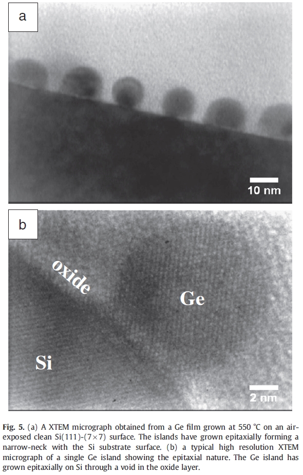
On the frontiers of nanotechnology, a revolutionary discovery has been made by a team of Indian scientists. The research led by Anupam Roy and B.N. Dev, published in the journal "Surface Science" with the title "Patterns in Ge cluster growth on clean and oxidized Si(111)-(7×7) surfaces," detailed the intricate process of growing germanium (Ge) nanoislands on silicon surfaces. This work not only unravels the secrets of self-assembly of nanostructures on silicon surfaces but also provides a crucial theoretical foundation for the design and fabrication of future nanoelectronic devices.
Nanoisle Formation and Molecular Beam Epitaxy
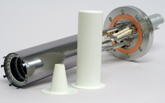
In the profound world of nanoscience, researchers employed precisely controlled molecular beam epitaxy (MBE) technology, coupled with advanced variable-temperature scanning tunneling microscopy (VTSTM) under ultra-high vacuum (UHV) conditions, to observe and analyze the growth behavior of Ge on silicon surfaces. The key to the experiment was to understand how Ge atoms deposit and form clusters on two vastly different silicon surfaces–one highly clean and the other oxidized. In MBE system, PBN crucible is applied by the researchers to maintain the high purity circumstance.

Impact of Surface Conditions on Nanoisle Growth
The experimental results revealed an intriguing contrast: on the unoxidized, clean silicon surface, Ge atoms tended to form nanoislands in specific regions with distinct boundaries, while on the oxidized silicon surface, Ge nanoisle formation was more dispersed, with a higher degree of freedom and less structural constraints. This finding is crucial for understanding the fundamental mechanisms of cluster growth under different chemical and physical conditions.
Mathematical Modeling Unveils Growth Dynamics
The research team developed a sophisticated reaction-diffusion model that revealed the dynamic mechanisms behind the nanoisle growth. The model incorporates surface defects as nucleation centers and describes the migration of Ge atoms on the silicon surface, as well as their interactions with the defects in the vicinity.
The Unique Contribution of PBN Crucibles
To achieve precise control over the deposition of Ge atoms, the research process utilized high-performance pyrolytic boron nitride (pBN) parts and pBN crucibles, known for their exceptional high-temperature and chemical stability, became an indispensable part of the experiment.
As a leading manufacturer of pBN crucibles in the market, QSAM Inc. provided the research team with professional customized services. The company's pBN crucibles, with their outstanding performance in terms of high-temperature resistance, corrosion resistance, and chemical stability, were well-suited for the MBE experimental environment.
Meticulous Experimental Design and Execution
The scientists used a precisely calibrated quartz microbalance to measure the mass of Ge deposited on the silicon substrate, allowing them to control the thickness of the Ge layer. This level of control was crucial for the success of the experiment, as it ensured the reproducibility of the results and provided valuable insights into the growth mechanisms. Additionally, the team employed real-time high-energy electron diffraction (RHEED) technology to monitor the growth process of the Ge nanoislands, providing dynamic information about the evolution of the nanostructure morphology.
Experimental Results and Future Applications
Through this comprehensive set of experiments, the scientists not only revealed the detailed process of Ge nanoisle growth on silicon surfaces but also demonstrated how to manipulate the size and distribution of the nanoislands by changing the experimental conditions. This research achievement opens up the possibility of integrating high-performance optoelectronic and electronic devices on silicon-based platforms, which can operate at smaller scales with higher efficiency and lower energy consumption.

The Power of Interdisciplinary Collaboration
The success of this research also highlights the importance of interdisciplinary collaboration. Physicists, chemists, materials scientists, and engineers worked together, combining their unique perspectives and expertise, to provide a comprehensive solution to the complex scientific problem.
Conclusion
The research by the Indian scientists not only offers a deep understanding of self-assembly processes at the nanoscale but also pushes the boundaries of nanotechnology. As this nanoisle technology continues to evolve and mature, we anticipate witnessing more innovative applications in the fields of electronics, optoelectronics, and quantum computing, enabling new breakthroughs.
