A Breakthrough in Growing High-Quality Gallium Arsenide Crystals
A Milestone in Gallium Arsenide Crystal Growth
Recently, the collaborative research findings of Min Jin, Jiayue Xu, Yongzheng Fang, Hui Shen, Guojian Jiang, and Zhanyong Wang from the Shanghai University of Science and Technology, along with Qingbo He from Chowin Photonics in Hangzhou, were published in the journal "Advanced Materials Research." The article, titled "Defects of GaAs Crystals Grown by the Pulling-Down Method," delves into the challenges encountered in growing gallium arsenide (GaAs) crystals using the pulling-down method, particularly the issue of crystal defects, and provides solutions to improve the overall quality of this semiconductor material.
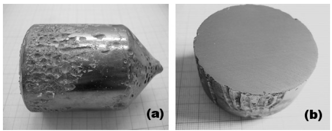
Gallium arsenide, an important III-V compound semiconductor material, holds an irreplaceable position in high-frequency, high-speed electronic and optoelectronic devices. The pulling-down method used in this study successfully grewdia2" GaAs single crystals, a technique originally used for the growth of oxide single crystals, now expanded to the growth of GaAs crystals, demonstrating its potential for producing high-quality crystals.
Observation and Analysis of Crystal Defects
The research team observed various defects in the grown GaAs crystals, including growth striations, small facets, pits, and dislocations. Through detailed analysis, the formation of these defects was attributed to multiple factors, such as the moisture content in the B2O3 encapsulant and the volatilization of arsenic due to the decomposition of GaAs. Specifically, the surface pits were directly related to the moisture content in the B2O3 encapsulant. Although "wet" B2O3 helps with the wettability of the crucible wall, the residual moisture vaporizes at high temperatures, leading to the formation of pits.

The Key Role of PBN Crucibles
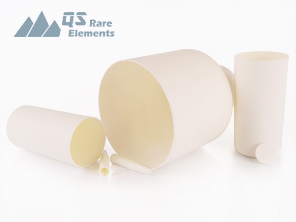
The experiments utilized PBN (pyrolytic boron nitride) crucibles to contain the 6N-purity GaAs polycrystalline feedstock and additional B2O3 encapsulant. PBN crucibles are commonly used materials in crystal growth, owing to their high-temperature resistance and other favorable properties. PBN crucibles played a crucial role in the GaAs crystal growth process, as they prevented the GaAs melt from directly contacting the crucible, avoiding undesirable chemical reactions or contamination.Notably, the formation of pits was also related to the moisture content in the B2O3 encapsulant. The researchers pointed out that "dry" B2O3 with lower moisture content might not be able to fully encapsulate the GaAs charge, leading to nucleation on the crucible wall and the subsequent formation of pits. In contrast, "wet" B2O3 with higher moisture content is expected to form a complete coating, which is beneficial for the wettability of the crucible wall, but the evaporation of residual moisture at high temperatures can potentially cause bubbles and pits on the crystal surface.

Growth Process and Quality Assessment
The GaAs crystals were grown in a pulling-down device, with the PBN crucible sealed in a quartz ampoule and evacuated before the growth process. The entire device included three temperature zones: a high-temperature zone for melting, a temperature gradient zone for crystal growth, and a low-temperature zone for annealing. The research used GaAs seed crystals and a closed-growth environment.
After KOH etching of the crystals, the measured etch pit density (EPD) was less than 5000 cm^−2, indicating that the pulling-down method can produce high-quality GaAs crystals. Additionally, some of the observed dislocations were in an arranged array, which may be due to a slight thermal stress distribution.
Despite the presence of defects, the research team concluded that the overall crystal quality is good. The study found that the pulling-down method can be a potential technique for growing high-quality GaAs crystals, which are crucial for various electronic and optoelectronic applications.
Research Support and Technological Frontier
This groundbreaking research was supported by the Shanghai Municipal Science and Technology Commission, the Hangzhou Municipal Science and Technology Bureau, the Shanghai Municipal Education Commission, and the Shanghai University of Science and Technology. The funding from these organizations has not only advanced the scientific exploration in the semiconductor materials field but also provided valuable knowledge resources for the industry.
Epilogue
PBN crucibles have proven to be crucial in ensuring the quality of crystal growth, and QSAM Inc., a leading manufacturer of PBN crucibles in the market, provides high-quality services to research users, helping them customize the high-standard crucibles they need. As semiconductor technology continues to progress, the demand for high-quality GaAs crystals will continue to grow, driving the advancement of electronics and optoelectronics. The success of this research marks a new starting point and lays a solid foundation for future technological innovations.
