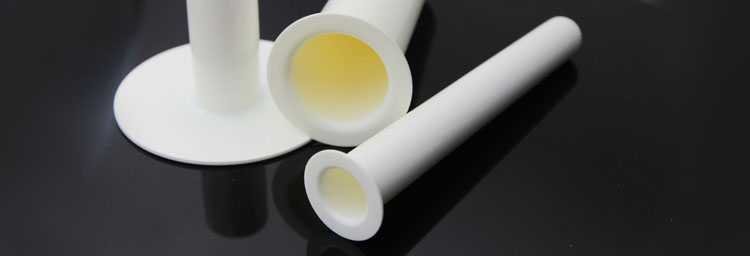
Introduction of MBE method
Introduction
The Molecular Beam Epitaxy (MBE) method is a well-established technique for growing highly crystalline thin films of various materials. It involves the deposition of atoms or molecules onto a substrate, under ultra-high vacuum conditions and low-temperature conditions. This process results in the formation of an epitaxial layer with good structural quality and precise control over thickness and composition. In this article, we will discuss the MBE method, some examples of its applications, and the use of PBN crucibles in MBE growth.

MBE Technique
The MBE technique is based on the Knudsen Cell principle, which states that atoms or molecules evaporated from a hot surface into a low-pressure gas phase travel through a vacuum towards a cold substrate where they condense into a thin film. The MBE method typically uses a high-purity source material that is heated by a resistive or electron-beam heater to create a beam of atoms or molecules directed towards the substrate, where they form a thin film. The system has multiple stages, including a loading chamber, a buffer chamber, a growth chamber, and a transfer chamber.
The growth rate and composition of the thin film are precisely controlled by regulating the temperature, pressure, and flux of source material. Monitoring these parameters enables the growth of complex multi-layer structures of different materials, such as semiconductors, metals, and oxides. The versatility of this method makes it an ideal choice for many different types of research applications, including basic physics, electronics, optoelectronics, and nanotechnology.
Applications
The MBE technique has found wide-ranging applications in the field of semiconductor research and device fabrication. One of the notable examples is the development of high-speed, high-frequency electronic devices such as Heterojunction Bipolar Transistors (HBTs). These transistors utilize GaAs-based heterostructures grown by MBE, offering a high carrier mobility, low noise figures, and excellent thermal stability.
Another significant application of the MBE method is in spintronics research. Spintronics is a field that exploits the intrinsic spin of electrons to achieve new types of electronic devices. The MBE method has played an important role in developing new materials with tailored magnetic properties, such as diluted magnetic semiconductors (DMSs), which are used in various spin-based devices.
MBE growth using PBN Crucibles
One critical component in this process is the crucible. The crucible is responsible for heating and evaporating the source material. Pyrolytic Boron Nitride (PBN) crucibles have become increasingly popular due to their unique thermal and mechanical properties. Below, we explore how PBN crucibles have contributed to the growth of MBE.
PBN crucibles exhibit several beneficial characteristics that make them highly suitable for MBE applications:
Chemically inert: PBN crucibles are resistant to chemical reactions, even in harsh environments. This property makes them ideal for growing materials that require high-temperature processing, such as III-V semiconductors.
High thermal conductivity: PBN crucibles conduct heat very efficiently, allowing for uniform heating and evaporation of the source material.
Low thermal expansion coefficient: PBN has an extremely low thermal expansion coefficient, meaning it does not change shape or size significantly when exposed to high temperatures. This property ensures that the crucible maintains its form and does not break or deform during the deposition process.
Non-wetting: PBN crucibles do not react or wet with most source materials, ensuring purity of the deposited material. As a result, high-quality, defect-free epitaxial layers can be grown.
Due to these advantages, PBN crucibles have gained popularity over traditional graphite or ceramic crucibles in MBE.

Overall, MBE growth using PBN crucibles has played a critical role in the development and applications of thin film technologies, such as in the production of semiconductor devices and electronic components for various industries. QS Advanced Materials Inc, as a supplier of advanced ceramics, is one of the leading supplier of PBN crucibles for both laboratory and manufacturing facilities. We can make crucibles of both small sizes, such as single ones that are only as big as a thumb with quantity 3 or 5ea, and large sizes with diameters exceeding 200mm. Send us your demand today for a quote. Custom designs are always welcome.
