Introduction to conductive ITO (Indium tin oxide) thinfilm
Transparent conductive oxide (TCO) is a kind of thin-film material with high transmittance and low resistivity in the visible spectrum range (380nm < λ < 780nm). TCO thin-film materials mainly include CDO, In2O3, SnO2, ZnO, and other oxides and their corresponding composite compound semiconductor materials

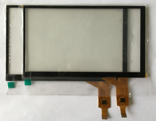
Development history: (1) in 1907, Baedeker et al. First prepared CDO transparent conductive films by a thermal evaporation method and began to study and utilize transparent conductive films. (2) transparent conductive films based on SnO2 and In2O3 were developed in the 1850s. (3) in the following '30s In this period, TCO materials are mainly based on these three systems: In2O3, SnO2, and ZnO. However, the properties of a metal oxide film can not meet the requirements of people because of the inherent physical properties of the material containing elements. In order to optimize the chemical and photoelectric properties of the films, and achieve high transmittance and low resistivity, scientists have done further research. (4) In the 1990s, some scientific research institutions in Japan and the United States started the research and development of multicomponent compound materials composed of more than two oxides. By adjusting the composition and chemical ratio, the TCO materials needed are obtained. At present, the most widely used TCO materials are indium tin oxide (ITO, In2O3: SN), aluminum-doped zinc oxide (azo, ZnO: Al), fluorine-doped tin oxide (FTO), SnO2: F), antimony doped tin oxide (ATO, sn2o: sb), etc. TCO is widely used in many fields, such as a transparent electrode, touch screen, flexible OLED screen, optical waveguide components, and thin-film solar cells.
In transparent conductive oxide films, ITO has high visible light transmittance, low resistivity (10-4 ~ 10-3 Ω· cm), good wear resistance, and stable chemical properties. Therefore, the proportion of Ito in TCO film is the highest. In general, ITO is a body-centered cubic ferromanganese structure, which is based on the doping of the In2O3 crystal structure. The In atom in In2O3 is six coordinated and the O atom is four coordinated. The intrinsic vacancy (oxygen vacancy) and Sn4 + substitution for in site contribute a lot of free electrons in the In2O3 crystal structure. Therefore, ITO is an n-type semiconductor with a carrier concentration of about 1021 / cm3, which is heavily doped.

The applications of ITO in various fields focus on the excellent properties of transparency and conductivity. The optical properties of ITO films are mainly affected by two factors: optical band gap width and plasma oscillation frequency. The former determines the spectral absorption range, and the latter determines the spectral reflection range and intensity. In general, ITO has high absorptivity in the short wave region, high reflectivity in the long-wavelength range, and the highest transmittance in the visible light range. Taking 100 nm ITO as an example, the average transmittance of 400-900 nm wavelength range is as high as 92.8%
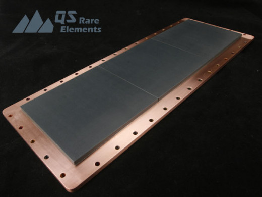
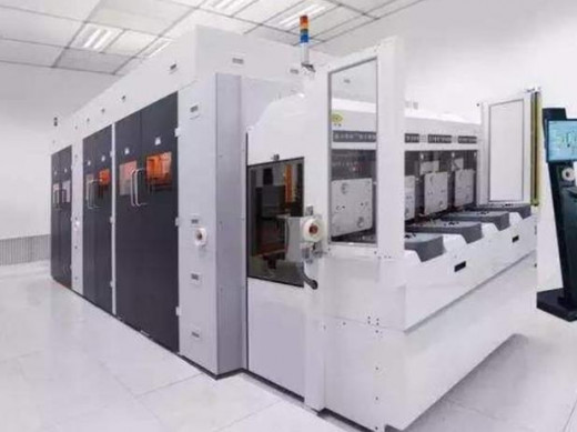
The properties of ITO films are mainly determined by the preparation process, and heat treatment is often used as an auxiliary means of optimization. In order to obtain ITO films with good conductivity, high transmittance, and smooth surface morphology, it is necessary to select appropriate deposition methods and optimize process parameters. The common coating methods include electron beam evaporation and magnetron sputtering. The main principle of electron beam evaporation: in a high vacuum environment, the high-energy electrons emitted by the electron gun bombard the surface of the ITO target under the action of the electric field and magnetic field so that the kinetic energy is converted into heat energy. The target material is heated up and becomes molten or evaporated directly, and the ITO film is deposited on the substrate surface. Magnetron sputtering belongs to the category of glow discharge. The film particles come from the cathode sputtering effect of argon ion on the cathode ITO target in a glow discharge. The target atoms are sputtered by argon-ion and deposited on the surface of the substrate to form the ITO film. To obtain high uniformity of the sputtered thin film of ITO, we need to make good control of the gas flow, electronic and magnetic fields and other factors. Check here for more information about different factors that could affect the uniformity of sputtering thin-film coating.

The upstream industrial chain of ITO is the manufacturing technology of raw material targets, which aims to obtain uniform and high-density green bodies. Improving forming technology is the key step to improve the quality of ITO target products. ITO target forming technology is generally divided into the dry method and the wet method. In essence, dry forming is a die pressing forming method, which is easy to realize automatic production. Moreover, under the action of pressure, the batch has a high density, which usually does not need to be dried. The dry forming process of the ITO sputter target mainly includes cold isostatic pressing forming, stamping forming, die pressing forming, and explosive forming. Wet forming is a process that uses the solution, solid-liquid mixture, gas-liquid mixture, and other raw materials to prepare the target material. The wet process needs drying treatment, with large deformation and shrinkage, more pores, and lower compactness. However, it can produce a large size and complex shape targets. Through a reasonable sintering process, ITO targets with high stability, high uniformity, and high density can be obtained. The wet process of the ITO target is mainly extrusion forming, gel casting, and grouting forming. The downstream industry of ITO is mainly the conductive glass technology in the flat panel display industry, that is, on the basis of sodium calcium-based or silicon boron-based glass substrate, a layer of indium tin oxide film is coated. In the flat panel display industry, it is used in the field of touch screens and LCD panels. Tp-ITO conductive glass is applied in the touch screen field, while LCD-ITO conductive glass is applied in the LCD panel field. The main difference between the two is that before ITO coating, LCD-ITO conductive glass will be coated with a layer of the silica barrier layer to prevent sodium ions from diffusing into the liquid crystal inside the cell.
Compared with other transparent conductive film materials, ITO has some disadvantages in many aspects. For example, ZnO film has the advantages of low cost, non-toxic, and pollution-free. However, due to the relatively late start of the research on ZnO, the overall photoelectric performance is worse than that of ITO film, so the ITO film based on indium oxide is still the most widely used in industrial production. In recent decades, the research on ITO thin films has focused on two aspects: one is the basic theoretical research of ITO materials, which involves the relationship between lattice constant and photoelectric properties of ITO films, the optimization of optimal doping, and the calculation of carrier upper limit, and the change of ITO bandgap width. On the other hand, the preparation methods of ITO are mainly explored
