ITO : From Sputter Targets to Smart Devices
Introduction of ITO
Indium tin oxide (ITO) proves extensively useful in electronics due to its unique optical and electrical properties. ITO combines the conductivity of tin dioxide and the transparency of indium trioxide. Let's explore ITO's characteristics, parameters, and applications - from sputtering targets to smartphones.
Firstly, ITO has a high density of 6.8 g/cm3. It also boasts a Young's modulus of 116 GPa for sputtered films with 10wt% tin dioxide. Furthermore, standard ITO exhibits electrical conductivity of approximately 1.3 x 10⁴ S/cm. Etching methods also vary - wet etching utilizes oxalic acid while plasma etching employs a gas mixture.
Sputtering ITO
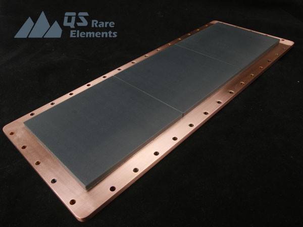
Key to many applications are ITO sputtering targets. As a composite of indium and tin oxides, high-quality targets exceed 99% density. This ensures properties such as minimized resistivity and maximized conductivity and strength. Such targets deposit onto substrates at lower temperatures. This creates transparent conductive films with reduced resistivity and enhanced transmittance for versatile uses.

ITO thinfilm
Devices with ITO
ITO enables two critical components. ITO films offer superb conductivity, transparency, hardness and stability. Widely applied in LCDs, PDPs, OLEDs, touchscreens, solar panels and more, films adjust light and resistance via indium-tin ratios.
Indium tin oxide film (ITO film) is a semiconductor transparent conductive film prepared through either vacuum evaporation or sputter deposition. ITO film offers not only high electrical conductivity but also high visible light transmittance. In addition, it exhibits excellent mechanical hardness and good chemical stability. As a result, ITO films see widespread use in manufacturing various electronic devices. Specifically, they are utilized in liquid crystal displays, plasma displays, electroluminescent displays, touch panels, solar cells, and more. Furthermore, the transmittance and resistance of ITO film can be controlled by adjusting the ratio of In2O3 to SnO2, which is typically 1:9.
Similarly, indium tin oxide conductive glass (ITO glass) involves depositing an ITO film layer onto soda-lime-based or silicon-boron-based glass through techniques such as sputtering or evaporation. Likewise, ITO glass finds extensive application in electronic displays. Specifically for LEDs, a silicon dioxide barrier layer is applied beforehand to prevent sodium ions from diffusing into the liquid crystal. Correspondingly, the substrates for LED ITO glass regularly employ ultra-float glass with characteristic tin surface ripples.
QS's ITO sputter target

ITO Sputter target
Moreover, QS Advanced Materials Inc. plays an important role as a supplier of various sputtering targets, including ITO targets. They cater to both the research and semiconductor industries. Likewise, they offer different molding methods for ITO sputter targets such as spraying, cold isostatic pressing, hot isostatic pressing, and wet forming. Consequently, obtaining these targets from QS enables the high-quality production of ITO films and ITO glass.
Summary
In conclusion, ITO plays a crucial role in the electronics industry, from its use as an ITO sputter target to the production of ITO films and ITO glass for a range of devices. QS Advanced Materials Inc. serves as a reliable supplier, providing a comprehensive selection of sputtering targets, including ITO, to meet the needs of research and semiconductor manufacturing.
