Breakthrough in Overcoming Key Challenges in GaN Crystal Growth
In the rapidly evolving semiconductor technology field, a team of researchers from the Central Research and Development Laboratory of a Japanese energy company (Inoue T., Seki Y., and Taguchi T.) and the Faculty of Engineering at Yamaguchi University (Kurai S. and Yamada Y.) have conducted a critical research project. They published a paper titled "Growth of Large-Sized Gallium Nitride Single Crystals by Pressure-Controlled Solution Growth under High Pressure" in the journal Physica Status Solidi (b), which details the development and validation of a new "Pressure-Controlled Solution Growth (PC-SG)" method, providing a more economical and efficient pathway for the production of high-quality GaN substrates.
GaN Material's Immense Potential and Growth Challenges
GaN-based optoelectronic devices have gained increasing attention due to their significant advantages in energy efficiency and performance. As a wide-bandgap III-V semiconductor material, GaN has extensive application prospects in areas such as optoelectronics and power electronics. However, the high melting point and high decomposition pressure of GaN have been the primary bottlenecks constraining the growth of GaN single crystals. Researchers urgently need to overcome this challenge to enable the widespread application of GaN materials in advanced electronic technologies.
Innovative Breakthrough in Pressure-Controlled Solution Growth
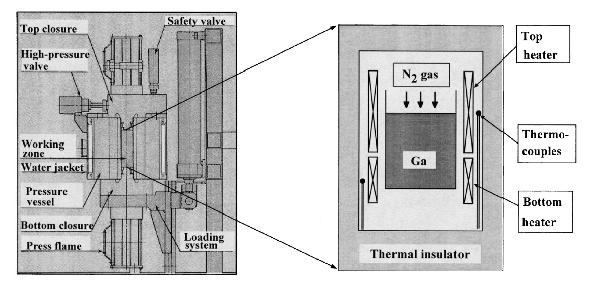
To address this, the research team developed a novel "Pressure-Controlled Solution Growth" method. Unlike traditional solution growth techniques, they applied supersaturated pressure at a constant temperature, avoiding issues such as solute supercooling, decreased growth rate, and solvent residue. By precisely controlling the nitrogen gas pressure and temperature using a high-pressure furnace (HPF#1), they successfully grew high-quality GaN single crystals within pBN (pyrolytic boron nitride) crucibles in a high-purity gallium solvent.

pBN Crucible - The Key Growth Container
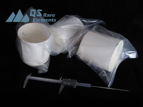
The pBN crucible played a crucial role in this experiment. This material has excellent thermal and pressure resistance, allowing it to stably contain the gallium metal and nitrogen gas under extreme conditions, making it highly suitable for high-pressure solution growth methods. During the PC-SG process, the gallium in the pBN crucible was heated under high-pressure nitrogen, promoting the supersaturation and crystal growth of GaN. By controlling the nitrogen pressure increase rate, the research team was able to grow GaN single crystals of different sizes and morphologies within the pBN crucibles, fully utilizing the advantages of pBN in providing a uniform nitrogen environment and maintaining stable growth conditions.

Fabrication of Large-Sized GaN Single Crystals
The experimental results showed that at 1475°C and 0.98 GPa nitrogen pressure, GaN single crystals could be grown by natural nucleation without any seeds. By adjusting the nitrogen pressure increase rate, the research team successfully obtained large-sized GaN single crystals with an area of up to 120 mm². The subsequent introduction of a new high-pressure furnace and multi-crucible system enabled the growth of GaN single crystals with an area of up to 300 mm², as well as the growth of 47 mm diameter GaN crystals on sapphire substrates. These achievements not only validate the exceptional performance of the PC-SG method but also inject new momentum into the commercialization of GaN-based devices.
New Hope Brought by Innovative Methods
Through the characterization of the obtained GaN single crystals using XRD, TEM, and PL, the researchers verified the effectiveness of the PC-SG method. This method not only can grow well-structured GaN single crystals under high pressure but also exhibits advantages in growth rate and crystal quality. The research team further proposed a new "Pressure-Controlled Liquid Phase Epitaxy (PC-LPE)" method, which holds promise for the low-cost manufacturing of high-quality GaN substrates, bringing new hope for the commercialization of GaN-based optoelectronic and power electronic devices.
As a leading manufacturer of pBN crucibles in the market, QSAM Inc. provided high-quality services to the research users. Their expertise in manufacturing and customized services enabled the researchers to obtain the most suitable high-quality crucibles based on their experimental requirements, supporting the in-depth progress of the scientific research.
Looking to the Future
The continuous innovation of Chinese scientists in the semiconductor materials field will undoubtedly inject new impetus into the development of China's electronic information industry. As the PC-SG and PC-LPE methods are further optimized and perfected, gallium nitride materials will play an increasingly important role in energy-efficient lighting, high-power electronics, and next-generation communication networks, leading the development of advanced electronic technologies. Through sustained innovation breakthroughs, China will become a high ground for key semiconductor materials, contributing Chinese strength to the global semiconductor industry.
