Breakthrough in Graphene Research: University of Tokyo Team Achieves High-k Oxide Integration
Recently, Nobuaki Takahashi and Kosuke Nagashio from the Department of Materials Engineering, University of Tokyo, collaborated with the Japan Science and Technology Agency (JST) PRESTO project and published a study on integrating high-k oxides on graphene using atomic layer deposition (ALD) technology. The research was published in the Applied Physics Express journal in 2016, titled "Buffer layer engineering on graphene via various oxidation methods for atomic layer deposition."
The Challenge of Gate Structures in Graphene Transistors
Graphene is widely regarded as a representative new material in modern semiconductor technology, with its exceptionally high electron mobility and mechanical strength, making it a promising candidate for field-effect transistors (FETs) and other electronic devices. However, the challenge of forming a reliable top-gate structure on graphene, especially the integration of high-dielectric-constant (high-k) oxides as the top-gate insulator, has been a technical hurdle.

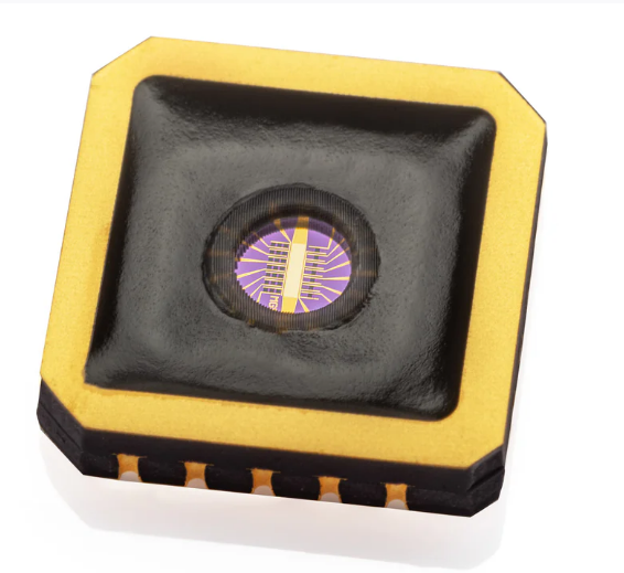
Graphene field-effect transistor mGFET-4P
Rare-Earth Element as a Buffer Layer
The research team chose yttrium (Y), a rare-earth element with high oxidizing capability, as the buffer layer. They explored different oxidation methods, including atmospheric pressure (AP) O2 annealing, high-pressure (HP) O2 annealing, and ozone annealing, to optimize the oxidation conditions for the top-gate insulator layer.
Key Experimental Steps
In the study, the researchers successfully improved the capacitance of the top-gate Y2O3 insulator layer and, under the application of an external electric field, the bilayer graphene showed a large on/off current ratio (Ion/Ioff ratio) after optimizing the conditions. The experiments also involved transferring monolayer graphene to a hydrophobic SiO2 surface, fabricating back-gate FETs with bilayer graphene, and depositing Y metal by thermal evaporation in an argon atmosphere using a PBN crucible.
The Critical Role of PBN Crucibles
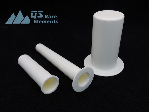
PBN (pyrolytic boron nitride) crucibles played a crucial role in this research. Due to their excellent thermal stability and chemical inertness at high temperatures, they became the ideal tool for metal thermal evaporation in an argon atmosphere. QSAM Inc., as a leading manufacturer of PBN crucibles in the market, provided high-quality customized services to the research team. Their expertise in PBN crucible manufacturing and customization enabled the researchers to obtain the most suitable high-quality crucibles, supporting the advancement of their scientific investigations.

Crucible
Precise Control under Experimental Conditions
During the thermal evaporation process in the argon atmosphere, the researchers were able to precisely control the deposition rate of the Y metal (around 0.1A/s) within the PBN crucible, which was essential for the subsequent oxidation treatment and high-k oxide deposition.
Research Outcomes and Challenges
The results showed that the thermal evaporation of Y metal as a buffer layer on graphene in an Ar atmosphere is feasible, as this method avoids the formation of defects in the graphene. Furthermore, the study found that the estimated dielectric constant of the Y2O3 thin film deposited by ALD on the buffer layer strongly depends on the oxidation degree of the buffer layer. While a large on/off current ratio was achieved, the researchers noted that the challenge remains to realize the ideal Y2O3 dielectric constant without introducing defects in the graphene.
Significance for the Electronics Industry
This research is crucial for understanding buffer layer engineering on graphene and the integration of high-k oxides, which is of great importance for advancing the development of graphene-based electronic devices. The study was supported by JSPS KAKENHI and the JSPS Core-to-Core Program, A. Advanced Research Networks.
Conclusion
The work from the University of Tokyo not only provides a feasible pathway for the practical application of graphene electronics, but also highlights the critical role of PBN crucibles in high-precision material deposition processes. As graphene technology continues to progress, we anticipate that these advanced research efforts will contribute to more revolutionary changes in the future electronics industry.
