
Innovative Breakthrough in High-Power Semiconductor Lasers by German Team Using Advanced Crucible Materials
Exceptional Materials Technology Guiding the Future of Laser Technology
In recent years, as technology has advanced rapidly, high-power semiconductor lasers have found increasingly widespread applications in industrial manufacturing, medicine, and telecommunications. The quality of the gallium arsenide (GaAs) substrate, which is a core component of these laser systems, directly impacts the performance and lifetime of the lasers. A research team from Germany has published their latest findings in the book "High-Power Diode Lasers," showcasing how advanced crystal growth techniques and material optimization can significantly improve the quality of GaAs substrates.
Research Collaboration
The research was jointly conducted by Georg Müller and Patrick Berwian from the Crystal Growth Laboratory of the Materials Science Department (WW6) at the University of Erlangen-Nuremberg, as well as Eberhard Buhrig from the Institute of Non-Ferrous Metallurgy at the Freiberg University of Technology. This interdisciplinary collaboration combined the expertise of materials science and metallurgy, driving innovation and application of the related technologies.
Innovation in Crystal Growth Techniques
In the manufacturing process of semiconductor lasers, the quality of the substrate material directly affects the efficiency and stability of the final product. To improve the quality of GaAs crystals, the research team employed the Vertical Bridgman (VB) and Vertical Gradient Freeze (VGF) techniques. These methods effectively optimized the growth quality of GaAs crystals by precisely controlling the temperature and chemical environment during the crystal growth process.
With the aid of the advanced computer simulation software CrysVUN++, the researchers were able to simulate the crystal growth process before the experiments, optimizing the design and operating parameters of the VGF furnace. This process helped to achieve a more uniform temperature distribution in the crystal growth environment, significantly reducing the dislocation density and improving the overall crystal quality.
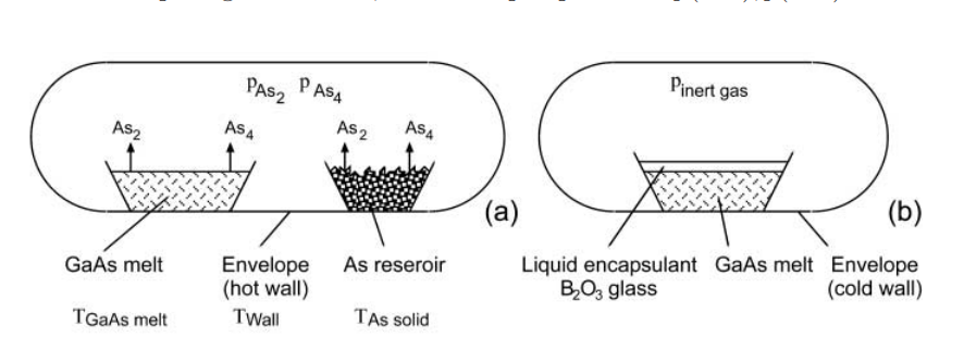
Hot wall principle (a) and body packaging principle (b)
The Key Role of pBN Crucible Materials
The choice of crucible materials is crucial in high-temperature crystal growth. The pyrolytic boron nitride (pBN) crucibles used in the research, with their high purity and excellent chemical stability, became the preferred material. The pBN crucibles not only can withstand high-temperature environments but also maintain their chemical properties, preventing the introduction of impurities and ensuring the purity of the crystal growth.
Additionally, the thermal conductivity and anisotropic thermal conductivity characteristics of pBN crucibles are also crucial for uniform crystal growth. These properties help the crucible maintain a stable temperature throughout the entire growth process, reducing temperature fluctuations and the resulting internal stresses within the crystal, further lowering the generation of dislocations.
QSAM Inc., as a leading manufacturer of PBN crucibles in the market, can provide high-quality services to the research community. Their professional manufacturing capabilities and customized services enable researchers to obtain the most suitable high-quality crucibles for their experimental requirements, supporting the advancement of scientific research.

PBN crucibles
Experimental Results and Future Outlook
By adopting the VB and VGF growth techniques, combined with high-quality pBN crucibles, the research team successfully reduced the dislocation density in GaAs crystals to 50 to 500 per square centimeter, a significant improvement compared to traditional growth techniques. This high-quality GaAs substrate is a key component in the manufacture of high-power, high-stability semiconductor lasers. Furthermore, the low-dislocation-density crystals not only improve the output efficiency of the lasers but also significantly extend their useful lifetime.
The team's achievement has garnered widespread academic attention and also brought practical benefits to the semiconductor laser manufacturing industry. In the future, this technology is expected to be widely applied in areas such as fiber optic communication, precision manufacturing, and medical treatment, enhancing the performance and reliability of related equipment.
Conclusion
The groundbreaking achievement of the German research team reflects the innovative potential of the cross-fertilization between materials science and metallurgy, as well as the important role of advanced materials and technologies in driving technological progress. Through continuous research and optimization of crystal growth techniques and crucible materials, future semiconductor lasers will become more efficient and stable, offering more possibilities for various industries.
Furthermore, this research emphasizes the importance of academic collaboration. By combining the expertise and resources of different disciplines and research institutions, the pace of technological innovation can be accelerated. As more such interdisciplinary projects are implemented, similar breakthroughs are expected to emerge in various high-tech fields.
Finally, with the sustained global demand for high-performance semiconductor devices, ongoing R&D investment and the commercialization of innovative achievements will provide a strong impetus for technological development and industrial upgrading. The research results of the German team not only contribute to the global progress of semiconductor and laser technology but also open new paths for the future development of the related industries, indicating a broader application horizon and market potential.