Breakthrough in Polariton Traps in GaAs Microcavities Enabled by PBN Crucibles
Recently, Joanna M. Zajac and Professor Wolfgang Langbein from the School of Physics and Astronomy at Cardiff University, UK, published a notable paper in Physical Review B titled "Structure and zero-dimensional polariton spectrum of natural defects in GaAs/AlAs microcavities". Their research reveals the origins of natural defects in GaAs microcavities grown by molecular beam epitaxy (MBE) system and explores the potential applications of utilizing these defects to create two-dimensional polariton traps.

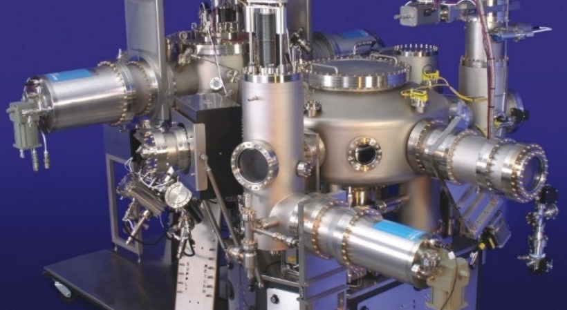
MBE System
GaAs/AlAs Microcavities: A Key Platform for Exploring the Polariton Realm
Semiconductor microcavities are an important platform for studying polariton physics, as they effectively confine the interaction between photons and semiconductor excitons, producing strongly coupled polariton states. These polaritons exhibit unique optical properties and may become crucial components for future polariton-based electronic and photonic devices.
In MBE-grown microcavities, natural defects often occur, which can significantly impact the optical properties of the polaritons. Joanna M. Zajac and Professor Wolfgang Langbein's research focuses on investigating the formation mechanism of these defects and their potential for controlling polariton states.
PBN Crucibles Enabling Experimental Precision
In their experiments, the researchers employed advanced characterization techniques such as focused ion beam (FIB) and scanning electron microscopy (SEM) to perform in-depth analyses of two microcavity samples (MC1 and MC2) grown at different temperatures. Notably, they chose to use pyrolytic boron nitride (PBN) crucibles as the container for the Ga source.
PBN crucibles have excellent high-temperature resistance, chemical inertness, and thermal conductivity, ensuring the stability and purity of the Ga melt during the growth process. As described, "Specifically, Ga cools near the orifice of the crucible and, since it does not wet the pyrolytic boron nitride (PBN) crucible surface, forms droplets which can fall back into the liquid Ga, causing a spatter of smaller Ga droplets." This Ga spatter behavior led to localized increases in the GaAs layer thickness, resulting in the formation of natural defects within the microcavity.

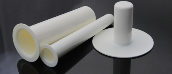
PBN Crucibles
Research Findings: Defect Origins and Control Potential
Through the detailed analysis of the MC1 and MC2 samples, the team led by Joanna M. Zajac and Professor Wolfgang Langbein made the following discoveries:
1. The defects originate from the spatter of the Ga source during growth, leading to localized increases in the GaAs layer thickness.
2. As the growth temperature increases, the defects become less elliptical in shape but larger in size, indicating that diffusion processes and Ga surface migration rates are key factors.
3. By combining various characterization techniques, including differential interference contrast (DIC) microscopy, FIB/SEM, and others, the research team comprehensively revealed the three-dimensional spatial structure of these defects.
4. These elliptical or circular natural defects exhibit localized polariton spectra, providing important insights for the design of novel polariton-based optoelectronic devices.
This discovery not only contributes to a deeper understanding of defect formation mechanisms in MBE growth but also opens up new possibilities for utilizing these defects to create two-dimensional polariton traps. In the future, polariton devices based on these unique defects hold great promise for applications in optoelectronics and quantum information processing.
QSAM Enabling Scientific Innovation
PBN crucibles are favored by scientific researchers because of their high temperature resistance, high chemical stability, non-reaction with experimental materials, and excellent thermal stability. As a major manufacturer of PBN crucibles, QSAM inc can provide this key tool to help researchers achieve precise control of experimental conditions and thereby obtain reliable research data.
QSAM will continue to focus on the research and production of PBN materials, providing even better experimental support for researchers and helping them achieve more breakthrough progress in the frontiers of polariton physics, novel optoelectronic devices, and beyond.
