Sputtering Thin Film Coating in Photovoltaic Applications
Sputter deposition is an important thin film coating technology in the field of photovoltaics. It allows for precise optimization of material properties to enhance solar cell performance. Thin film coatings are applied to photovoltaic materials using sputtering for several key reasons.
Why use sputtering
Firstly, coatings can maximize light absorption. Sputtering deposits films with specific thicknesses and refractive indexes. This allows for customized optical properties to absorb more sunlight and boost energy conversion efficiency. Coatings also aid electrical characteristics. The sputtered films increase conductivity and charge mobility within solar cells.

A sputter chamber with multiple target mount
The sputtering process involves ion bombarding a target material in a vacuum chamber. High-energy ions eject atoms from the target, which then deposit as a uniform thin film onto the substrate. Researchers can accurately control factors like thickness and composition. This makes sputtering suitable for high-quality coatings.
Common sputtering targets for photovoltaics include
Cadmium telluride is used in thin film solar cells due to its absorption and low costs. CdTe targets deposit films on substrates to create efficient cell structures. The coatings absorb visible and infrared light well for photovoltaic applications.
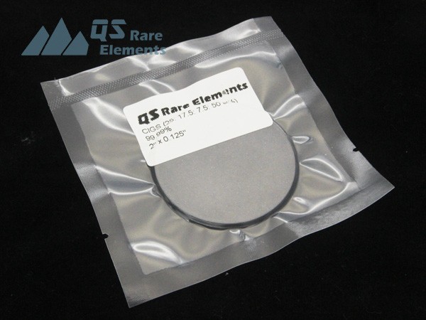
Copper indium gallium selenide is a versatile and efficient thin film material. CIGS sputter targets form absorber layers on substrates. The sputtered films exhibit strong absorption and can be fabricated at relatively low temperatures, allowing flexibility.

CIGS sputter target (QS Rare Elements is the former name of QS Advanced Materials)
Gallium arsenide is employed in concentrated photovoltaic systems where high efficiency is crucial. GaAs targets assist in developing solar cells with excellent performance under concentrated sunlight.
QS Advanced Materials supplies a range of sputtering targets. Our production tools like vacuum induction melting and hot pressing enable custom-shaped flat disc targets up to 18 inches in diameter. QS also caters to researchers through small test samples. Our sputter targets serve the photovoltaics and research sectors reliably.
Summary
sputter deposition coatings are instrumental in optimizing solar cell performance through enhanced absorption and electrical characteristics. QS Advanced Materials supplies the sputtering targets that drive these photovoltaic material improvements through precise thin film engineering.
