Tin (Sn) Sputtering Targets
Composition: Tin
Catalog No.DPME50ST
Purity:99.9% ~ 99.999%Please click ![]() for discount and other size
for discount and other size
- Product Details
Tin (Sn) sputtering target specifications
Formula: Sn
CAS No.: 7440-31-5
Max. dia. of flat disc sputter target: 18"
Typical lead time of Sn sputtering target:2 weeks
Regular Dimensions and Price of Tin (Sn) Sputtering Target
| Product Name | Reference Price | |
| 2"diax 1/8"t Tin sputtering target | $260.5 | Add to Chart |
| 3"diax 1/8"t Tin sputtering target | P.O.R. | Add to Chart |
| 2"diax 1/8"t Sn sputtering target with In bonding to Cu bck plt | $341 | Add to Chart |
| 3"diax 1/8"t Sn sputtering target with In bonding to Cu bck plt | P.O.R. | Add to Chart |
About Our Sputtering Target
QSAM is a professional supplier of custom manufacturered R&D consumptions. Our equipment setup are flexible to meet various demands from wide range of customers for flat disc sputter targets. We are supporting US national labs and worldwide univeristies and researching facilities with our target material and other customized product. Please check here for the list of our other Single Element sputter targets
About Tin
Tin is a soft, silvery-white metal with a low melting point and good electrical conductivity. It is widely used in various electronic applications due to its versatile properties. Tin is a key component in lead-free solders, which are essential for the assembly of electronic devices. These solders provide reliable electrical connections while meeting environmental and health regulations. Tin oxide (SnO2), a transparent conducting oxide (TCO) material, finds extensive applications in optoelectronic devices, such as solar cells and displays. Sputtering techniques have been employed to deposit tin and its compounds, including SnO2, enabling the fabrication of high-quality thin films with desired properties. Tin sulfide (SnS) and tin selenide (SnSe) have also been investigated for their potential in photovoltaic and thermoelectric applications, where they can be deposited as thin films using sputtering methods. The ability to control the composition, thickness, and microstructure of tin and its compounds through sputtering has greatly advanced the development of electronic and optoelectronic devices.;
Tin Sputtering Target Packaging
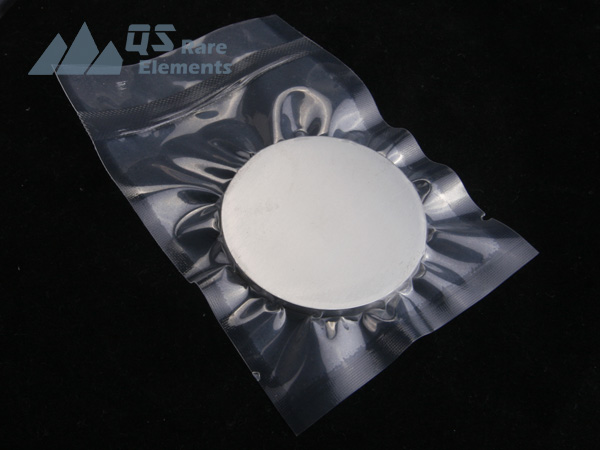
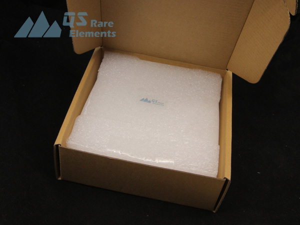
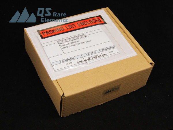
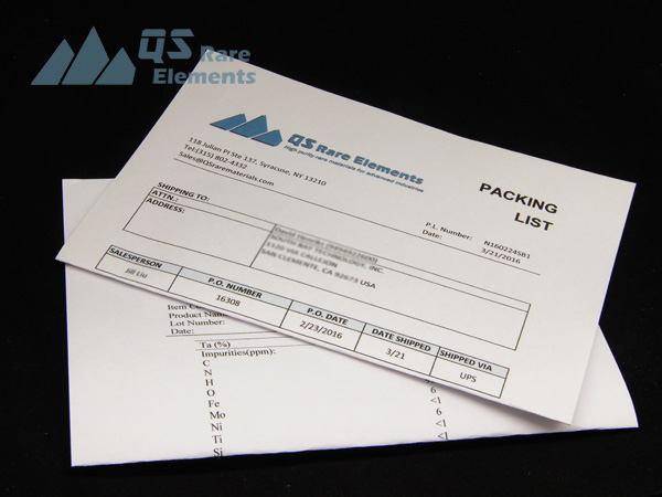
QSAMs sputter targets are vacuum sealed in plastic bags for shipping. We also use heavy foam to protect it. Common documents together with the sputter targets are packing list and analytical report e.g. COA


Related Product

