Tin Sulfide (SnS2) Sputtering Targets
Composition: Tin Sulfide (SnS2)
Catalog No.DPSF50ST
Purity:99.9%Please click ![]() for discount and other size
for discount and other size
- Product Details
Tin Sulfide (SnS2) sputtering target specifications
Formula: SnS2
CAS No.: 1315-01-1
Max. dia. of flat disc sputter target: 8"
Typical lead time of SnS2 sputtering target:5 weeks
Regular Dimensions and Price of Tin Sulfide (SnS2) Sputtering Target
| Product Name | Reference Price | |
| 2"diax 1/8"t Tin Sulfide sputtering target | $929 | Add to Chart |
| 3"diax 1/8"t Tin Sulfide sputtering target | $1,173 | Add to Chart |
| 2"diax 1/8"t SnS2 sputtering target with In bonding to Cu bck plt | $1,009 | Add to Chart |
| 3"diax 1/8"t SnS2 sputtering target with In bonding to Cu bck plt | $1,308 | Add to Chart |
About Our Sputtering Target
QSAM is a professional supplier of custom manufacturered R&D consumptions. Our equipment setup are flexible to meet various demands from wide range of customers for flat disc sputter targets. We are supporting US national labs and worldwide univeristies and researching facilities with our target material and other customized product. Please check here for the list of our other Sulfides sputter targets
About Tin Sulfide
Tin disulfide (SnS2) is a layered semiconductor belonging to the family of metal dichalcogenides. It possesses a hexagonal crystal structure and exhibits unique electronic and optical properties. Thin films of SnS2 can be deposited using sputtering techniques, allowing for the fabrication of uniform and well-controlled layers. These sputtered SnS2 films have been explored for their potential applications in various optoelectronic and electronic devices. In particular, SnS2 has shown promise in the development of photodetectors, where it can efficiently convert light into electrical signals. Its layered structure and suitable bandgap make it sensitive to a wide range of wavelengths, from the visible to the near-infrared region. Additionally, SnS2 has been investigated as a component in solar cells and lithium-ion batteries, where it can enhance the performance and stability of these devices. The ability to deposit high-quality SnS2 films by sputtering has greatly facilitated the study and application of this material in diverse fields. Sputtering offers precise control over the composition, thickness, and morphology of SnS2 films, enabling the optimization of their properties for specific applications. Moreover, the scalability and reproducibility of sputtering processes make it a promising technique for the large-scale production of SnS2-based devices. As research continues to unveil the full potential of SnS2, sputtering will likely play a crucial role in the development of advanced optoelectronic and energy storage technologies based on this fascinating material.;
Tin Sulfide Sputtering Target Packaging
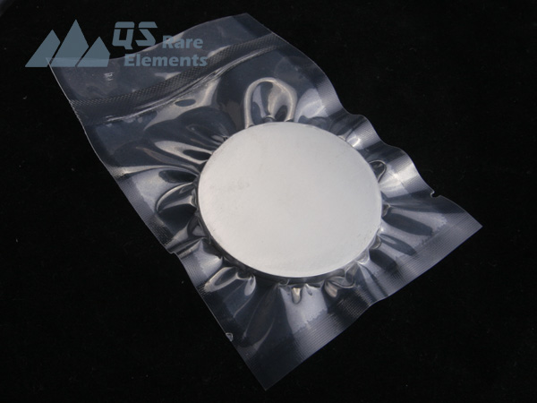
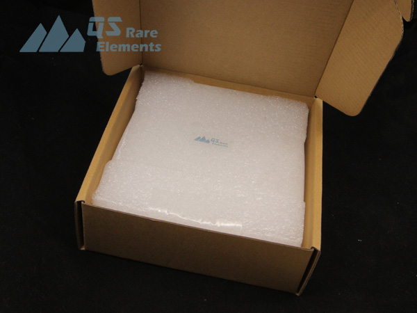
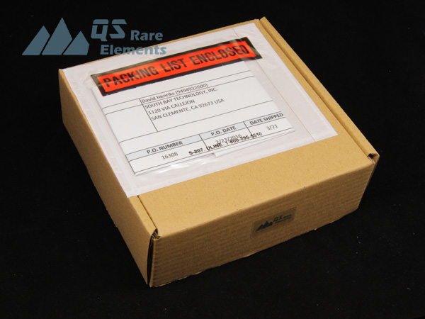
QSAMs sputter targets are vacuum sealed in plastic bags for shipping. We also use heavy foam to protect it. Common documents together with the sputter targets are packing list and analytical report e.g. COA


Related Product

